Panneaux solaires haut rendement
Crédits : CEA

High-efficiency photovoltaics

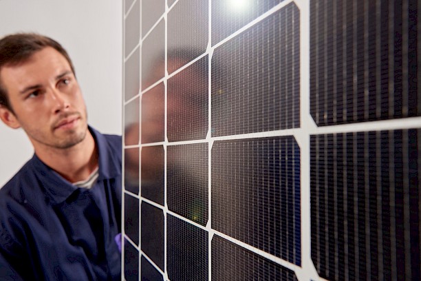
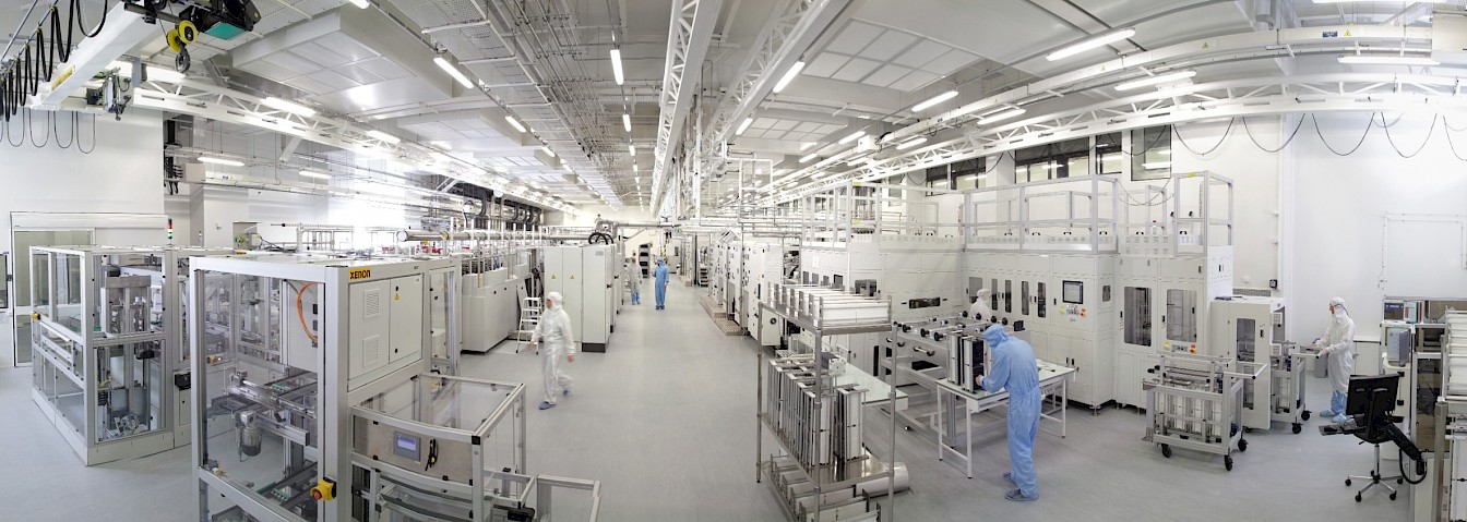
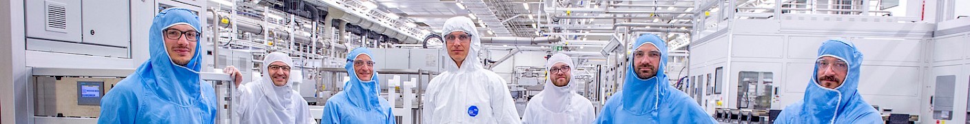
The CEA at INES is developing competitive and promising technologies for the years to come. Research activities mainly concern photovoltaics based on silicon, cells and modules, and the advanced processes to produce them. They focus on two major challenges:

  • Achieving the best energy efficiency with 25% efficiency on silicon and 30% with tandem cells.
  • Continuing to reduce costs to ensure the competitiveness of innovations and to achieve an increasingly competitive cost of solar electricity.

Achieve 25% efficiency with industrial heterojunction technology

The global photovoltaic industry is witnessing the emergence of high-efficiency technologies such as Silicon Heterojunction Technology (SJT), also known as "SJT" for "Silicon heterojunction". It offers key advantages: high conversion efficiency, favorable temperature coefficient, simple process compatible with competitive production costs, and the ability to make bifacial panels improving final productivity.

For more than 10 years, the CEA at INES has been developing heterojunction technology and is now in a unique position on the international stage to disseminate this technology through its "LabFab HET" pilot unit. This research tool enables our teams to validate high performance processes (up to 2,400 wafers per hour) and to set performance records that can be rapidly applied to industry.

Passivated contacts and advanced processes for high-efficiency photovoltaics

Passivated contacts based on ultra-thin polysilicon on SiOX oxide have become a key element in the landscape of high-efficiency photovoltaic solar cells. These structures are used both in single junction devices for the electrical passivation of metal/silicon interfaces, and in multi-junction cells for the development of "passivating" interfaces between sub-cells.

The CEA at INES leads research in order to understand the associated physical mechanisms and to master the processes of elaboration of these structures, and all other technologies leading to high performance. Since 2016, it has gained international recognition for these technologies.

Towards 30% efficiency with Perovskites and tandem cells

The photovoltaic efficiencies achieved today by silicon technologies are close to the theoretical limits that can be reached. New device architectures must be investigated in order to further increase the efficiency of the cells towards 30% and thus the price of the electricity produced. Tandem architectures combining silicon and perovskite cells seem to be the best candidates to meet these objectives.

The CEA at INES, which has demonstrated its ability to take laboratory results to industrialization for heterojunction silicon cells, for printed technologies such as organic photovoltaics, is now tackling the challenge of single-junction perovskite cells and for tandem perovskite cells on silicon.

Innovative panel architectures and manufacturing process

To find competitive margins, the photovoltaic industry is constantly innovating with new photovoltaic panel architectures, new ways of interconnecting cells and new materials. Everything is being done to further increase efficiency and power. This industry can also benefit from implementing new methods to move towards the manufacturing plant of the future.

The CEA at INES is developing innovative tools for the development of photovoltaic panels and how to produce them :

  • Through new methods for the field such as numerical modeling
  • By formats, such as cut-out cells, or recent architectures/concepts such as bifacial panels or cell tiling
  • Through the development of advanced equipment and processes

Platform and facilities of excellence

- The "LabFab HET" pilot line hosts the developments of heterojunction technology and their pre-industrialization. It allows for example to validate new processes at speeds relevant to the industry of 2400 cells per hour. This near industrial unit could produce 30 MW per year operated in industrial conditions.

- The RESTAURE research platform and its 1200 m² of white rooms has a range of manufacturing or characterization equipment enabling it to address all types of photovoltaic cell architectures on silicon.

- The Perovskites platform allows photovoltaic technologies using printed processes such as perovskites to move to large surfaces, in a controlled particle, temperature and humidity environment. Its close proximity to the RESTAURE platform allows for optimal tandem cell development.

- The Modules platform offers all the necessary versatility on 1500 m² and is equipped with industrial-type equipment to shorten the transfer to industry as much as possible.

Website made with  et  éco-conçu pour diminuer son empreinte environnementale.
Angle Web, Website eco-design in Savoie