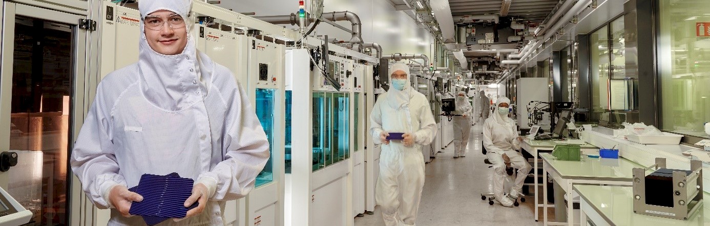
Crédits : D. Guillaudin - CEA
RECORD heterojunction cell with P-type silicon
Published on 03/24/2022
Within the framework of the strategic partnership between CEA INES and Enel Green Power for the industrialisation of heterojunction cell technology in Europe, our teams have already achieved an efficiency of 25%.[1]
To achieve such performance, the crystalline silicon wafer must be of very high quality, the preferred choice being N-type wafers doped with phosphorus and obtained by Czochralski pulling. Cells manufactured in this way are less sensitive to metallic impurities. They are also not affected by the light degradation phenomenon associated with Boron-Oxygen complexes (BO-LID), which is known to significantly reduce the electronic performance of Boron-doped P-type Cz wafers.
P-type wafers, which are the most widely used in the world, benefit from a lower cost.
A new way of manufacturing P-type Cz wafers has recently been deployed on a large scale by replacing boron doping with gallium (Ga) doping at no extra cost, making them insensitive to degradation phenomena under light. A recent study[2] indicates that P-type heterojunction cells should have an efficiency gap of less than 0.4% absolute to be competitive with N-type heterojunctions.
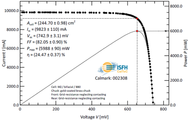
The use of Ga-doped wafers for the production of P-type heterojunction cells by the CEA teams at INES and Enel Green Power has led to a new milestone: a world record of 24.47% for a P-type silicon heterojunction cell with an industrial surface. This was achieved using the same manufacturing processes as the N-type, demonstrating once again the versatility and robustness of this technology.
The result, certified by ISFH Caltec, is to our knowledge the 2nd highest efficiency[3] for industrial size silicon cells based on the use of a P-type silicon wafer of any technology. LONGi Green Energy Technology, a world leader in the manufacture of these materials, made the wafers. More details will be announced at the 8th World Photovoltaic Power Conversion Conference WCPEC in Milan in September 2022.
2-N.L. Chang et al. “The Technical and Economic Viability of Replacing n-type with p-type Wafers for Silicon Heterojunction Solar Cells”, Cel Rep. Phys. Sci.2020, 1, 100069.
3- M. A. Green et al., Prog Photovolt Res Appl.2022;30:3–12 - https://www.longi.com/en/news/7056/